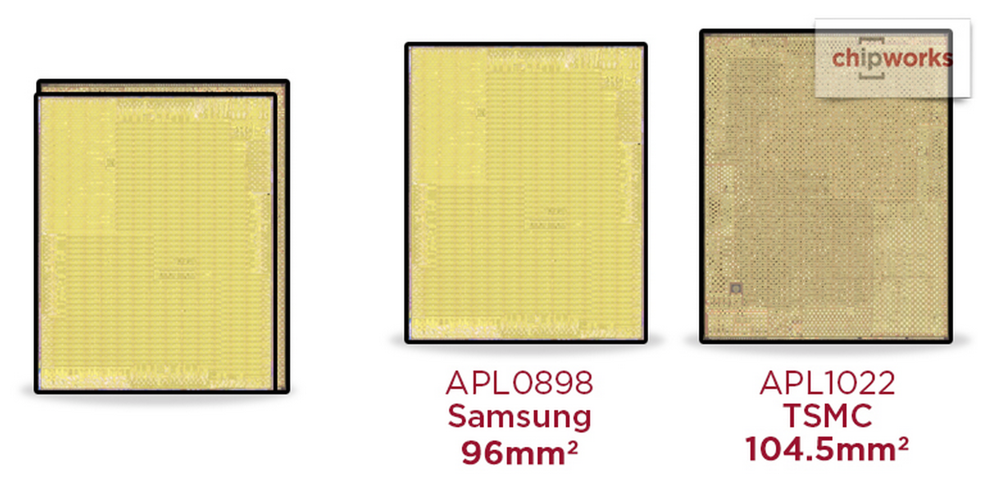
According to Chipworks, there are actually two different sized A9 processors floating around in the iPhone 6s and 6s plus released last week. That’s not really a surprise because Apple likes to have redundancy, especially when one of the manufacturers is Samsung. We’d heard that both Samsung and TSMC would be producing A9 processors destined for the iPhone 6s.
However, there appears to be a difference in size of the two A9s which might play a role in how the iPhone performs…
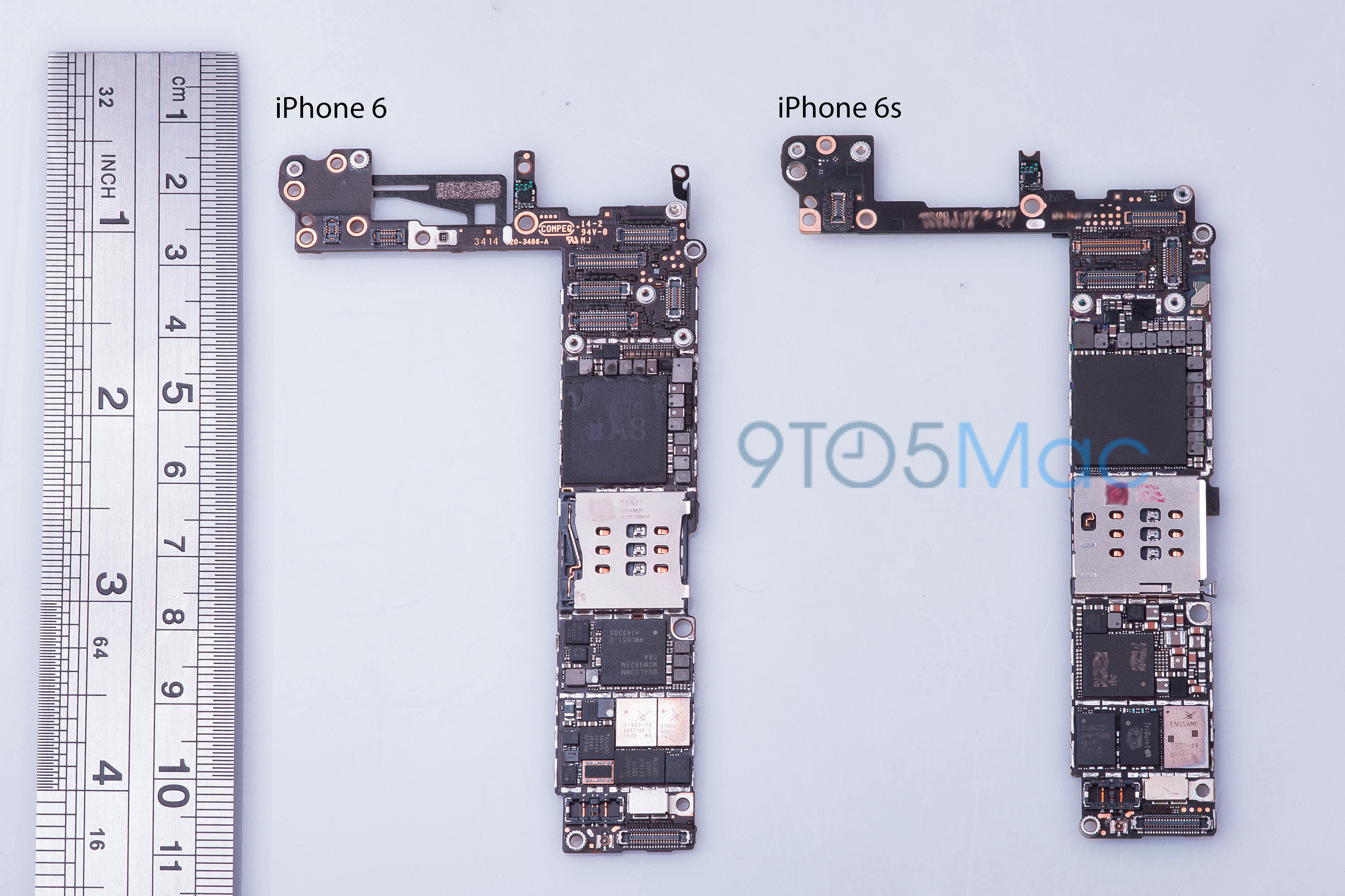
Our look at the upcoming “iPhone 6S” continues today with a discussion of new internal components that are expected to be inside Apple’s latest smartphone. In addition to expected changes such as a Force Touch display, upgraded camera system, and new Qualcomm LTE chip for up to twice-as-fast data speeds, the next iPhone will likely include updated NFC hardware, fewer and more efficient chips, and new flash memory that may nonetheless remain at a 16GB minimum capacity.
Nearly two weeks after the product’s official release, Chipworks has updated its earlier Apple Watch teardown to note several significant details, most notably that Apple’s latest processor uses a 28-nanometer building process that has already been leapfrogged by newer technology. The discovery reveals that the S1 — believed to be roughly equivalent in processing power to Apple’s A5 processors — can be readily evolved using the smaller 20-nanometer process used in Apple’s current A8 processors, as well as the cutting-edge 14-nanometer process that’s reportedly being used in the upcoming A9. This is good news for next-generation versions of the Apple Watch, as they will be able to easily fit faster or more power-efficient processors in the same space as the S1.
As highlighted in separate chip teardown and X-ray analyses released today by Chipworks and iFixit (partnered with Creative Electron), the S1 packs over 30 components into a resin-covered package, including everything from wireless chips, wireless charging, audio processors and sensors to the CPU itself. The CPU is again said to be Samsung-fabricated, continuing the unusual frenemy relationship between Apple and one of its chief consumer electronics rivals. Several of the beautiful iFixit/Creative Electron X-ray images of the Apple Watch are included below…
There has been a lot of controversy over Apple’s new Lightning connector introduced with the iPhone 5 and refreshed iPod lineups. Perhaps the biggest source of frustration for users and accessory manufacturers alike is the inability, so far, to produce official third-party products using the new standard. Apple has yet to update accessory makers with changes to its ‘Made For iPad/iPhone/iPod (MFi)’ policies. This will apparently require approval of facilities manufacturing Lightning products, but according to reports, it will not come until at least next month.
For accessory makers wishing to produce unofficial Lightning products, that process has proven difficult thanks to chips Apple has built into the connector thought to include security features. Despite reports that the security features have already been reverse engineered, and one or two third-party products on the market using the original Lightning cables from Apple’s suppliers, we have yet to experience a flood of Lightning products available to consumers. We also did not know exactly what tech Apple is including in these chips, something that we get a better look at today courtesy of a detailed teardown from Chipworks.
Once inside, Chipworks found a TI chip labeled “BQ2025” (alongside a handful of others) that could possibly include security features. The chip isn’t listed on TI’s website, but four similar chips are:
However, TI does have published datasheets on the BQ2022, BQ2023, BQ2024, and BQ2026. These four chips are cataloged on TI’s website as battery fuel gauges, but they are not identical, with three of them being serial EPROMs and one of them being a battery monitor IC… All use a single wire SDQ interface (TI’s proprietary serial communications protocol), and all have some basic security features such as CRC generation. So, it is certainly likely that the BQ2025 does have some security implemented on it. It would also seem likely that it includes an SDQ
Another possibility is that the chip is being used to better conserve electricity. For example, the cable could stop drawing electricity once the connected iOS device is fully charged to provide the obvious benefit of saving power. According to research from Opower, the iPhone 5 costs a mere 41 cents annually to charge once per day. However, the focus might simply be a greener, more energy efficient product.
In terms of the security features, Chipworks noted this is “the first secure cable” it has seen with this type of security device. It also speculated that, in terms of Lightning connectors, “piracy is not a concern” for Apple:
When Apple introduced the iPhone 5, Senior Vice President of Worldwide Marketing Phil Schiller noted a number of new methods being used for noise cancellation from solutions using the device’s third microphone to an updated “noise-cancelling earpiece” and the addition of wideband audio. We know from reports earlier this month that Apple is not including noise cancellation technology from Audience, as it did in previous iPhone models. While we do not know exactly what powers the iPhone 5’s enhanced audio system, Chipworks discovered a second Cirrus chip being used in its recent teardown:
Audio chips from Cirrus. We know that Audience announced that they no longer have the noise cancellation and we were hoping we could get a little insight as to what is being done in the iPhone 5. Unfortunately, without a little more depth than a die photo can provide the best we can say is that Cirrus has two design wins related to the audio (one of which we originally guessed to be a memory MCP). One has some fairly large transistors and a whole lot of logic. If someone out there knows what the Apple package 338S1077 is we would be happy to report it. Starting here may be a good place.
Apple 338S1077 Audio CODEC. This is a wafer-scale device by Cirrus Logic. They have long held this private-label package with Apple.
Apple 338S1117 Cirrus Audio Chip
It is very possible that Apple’s new, in-house noise canceling technology uses this new Apple-branded Cirrus chip. Expand Expanding Close
iFixit is hardcore when it comes to breaking open our favorite electronics to see what’s inside, and the website did it again today with the new Apple EarPods that just unveiled last week.
There is no repairability score for the EarPods, because they are “the throw-away kind.” Due to their glue blinding, iFixit warned the EarPods would never be the same if taken apart. In fact, an X-Acto blade was needed to cut the headphones open.
The notable tidbits from inside:
The EarPod speakers house a diaphragm/ paper cone, a voice coil, a permanent magnet, and a cabinet. Previous Apple headphones used plastic cones rather than paper.
The new design includes “larger cable wrapping on both ends” to sustain durability and minimize strain on the wires, and Apple removed the external microphone grate to make the EarPods more resilient to moisture damage.
As for the EarPod remote microphone:
The microphone in the EarPods’ remote bears the markings 2F17 045; we also uncovered another IC with the markings TI25ASGVI, which Chipworks believes to be an ADC, or a device used for volume-control duty.
Oh, and click here to see a size comparison of the remote’s circuit board alongside a U.S. dime.
Something to consider: Perhaps the new EarPods are so “mediocre'” because Apple wants to protect ears from the type of sound that only plug earphones produce. Apple sells many headphones, so producing a good sound that protects ears is probably a high priority for the oft-sued Apple.
ChipWorks and iFixit are hardcore when it comes to breaking open our favorite devices to see what is inside. The two websites decided to take it up a notch today by joining forces to publish a live teardown of the non-LTE Samsung Galaxy SIII. ChipWorks looked at the—you guessed—chips, while iFixit focused on repair aspects.
Yep, that is Samsung’s Exynos 4412, 32 nm CMOS, 1.4 GHz quad core ARM processor.
“The Exynos is in a standard PoP (Package-on-Package) assembly with a Samsung LP DDR2 Green Memory K3PE7E700M-XGC2,” explained ChipWorks. “It is notable that this is the same process generation as we documented in the Apple A5 rev 2, APL2498, also fabricated by Samsung and for which you can see the general structure.”
The device also features the Sony IMX145 is an 8-megapixel, 1.4 um pixel pitch, back illuminated CMOS image sensor. Sony designs and manufactures this image sensor, which the Apple iPhone 4S also boasts. Samsung provides its own storage, however, with the KMVTU000LM. According to ChipWorks, it is a multi-chip Samsung MOVI N and memory module.
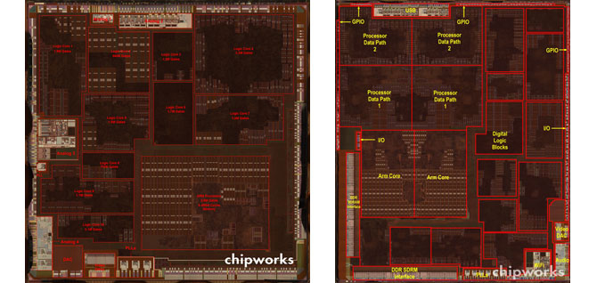
Floorplan comparison: Apple’s A4 chip (left) and the latest A5 processor (right)
Reverse engineering wizards over at Chipworks put the A5 chip under a microscope. Yes, it’s a Samsung – confirming our hunch. The experts came to this conclusion by putting the chip under a microscope and examining dielectric layers and the shape of the transistor gates. The teardown analysis also revealed a die almost twice the size of the A4 chip from the previous-generation iPad and iPhone 4, the 45-nanometer manufacturing process and other interesting tidbits.


 For accessory makers wishing to produce unofficial Lightning products, that process has proven difficult thanks to chips Apple has built into the connector thought to include security features. Despite reports that the security features have